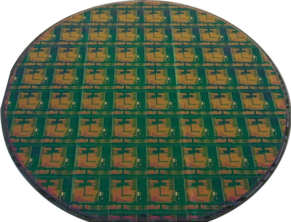
TAVI is a generic and cost-effective industrial platform for the development of customized InP PICs.
The platform supports product development through the entire cycle, from prototype to volume manufacturing.
TAVI is a generic and cost-effective industrial platform for the development of customized InP PICs.
The platform supports product development through the entire cycle, from prototype to volume manufacturing.
Are you developing optical modules requiring high speed modulation or detection?
Are you developing optical modules requiring high speed modulation or detection?
Do you need any light source or gain block chip for your silicon photonics device?
Do you need any light source or gain block chip for your silicon photonics device?
Do you need any light source or gain block chip for your silicon photonics device?
Do you need any light source or gain block chip for your silicon photonics device?
If no one can offer you an industrial grade and cost-effective solution, that can deliver on time, and reach large volumes… We are your light!
If no one can offer you an industrial grade and cost-effective solution, that can deliver on time, and reach large volumes… We are your light!
MAIN PHOTONIC INTEGRATION APPLICATIONS

Datacom and Telecom transceivers and Co-packaged Optics
Custom InP chips for:
• Optical light generation and detection subsystems and modules in telecom and datacom.
• Pluggable Tx/Rx/TxRx modules for datacenter optical interconnects, on-board optics and co-packaged optics.
Datacom and Telecom transceivers and Co-packaged Optics
Custom InP chips for:
• Optical light generation and detection subsystems and modules in telecom and datacom.
• Pluggable Tx/Rx/TxRx modules for datacenter optical interconnects, on-board optics and co-packaged optics.
Hybrid Photonic Integration
Custom lasers and gain elements (semiconductor optical amplifiers, SOAs) for hybrid integration with silicon photonics (silicon-on-insulator, silicon nitride, and PLC technologies).
Hybrid Photonic Integration
Custom lasers and gain elements (semiconductor optical amplifiers, SOAs) for hybrid integration with silicon photonics (silicon-on-insulator, silicon nitride, and PLC technologies).


RF Photonics and Quantum
Custom RF PICs for on-chip generation, processing and detection of high-frequency RF signals for applications like microwave photonics, 5G, frequency generation, up/down-conversion, quantum key distribution (QKD), quantum random number generation (QRNG), quantum computing.
RF Photonics and Quantum
Custom RF PICs for on-chip generation, processing and detection of high-frequency RF signals for applications like microwave photonics, 5G, frequency generation, up/down-conversion, quantum key distribution (QKD), quantum random number generation (QRNG), quantum computing.
TAVI PHOTONIC INTEGRATION TECHNOLOGY
TAVI stands for Taper-Assisted Vertical Integration, and the technology is based on:


Monolithic photonic integration in InP
Vertical integration
Evanescent-field coupling
Regrowth-free process
Epitaxy and fabrication are decoupled and can be delivered independently


TAVI OFFERING FOR CUSTOM PICs
Designs compatible with the commercially available and yet decoupled epitaxial growth and regrowth-free wafer fabrication processes.
Designs compatible with the commercially available and yet decoupled epitaxial growth and regrowth-free wafer fabrication processes.
Comprehensive library of pre-verified and standardized functional waveguides and devices/components formed with them, a.k.a. building blocks.
Comprehensive library of pre-verified and standardized functional waveguides and devices/components formed with them, a.k.a. building blocks.
Industrial grade wafer fabrication foundry: mature process, clear design rules, 24/7 operations controllable yields.
Industrial grade wafer fabrication foundry: mature process, clear design rules, 24/7 operations controllable yields.
World’s #1 independent epitaxy supplier: known good wafers, low-risk and on-time epitaxy procurement.
World’s #1 independent epitaxy supplier: known good wafers, low-risk and on-time epitaxy procurement.
World’s #1 independent epitaxy supplier: known good wafers, low-risk and on-time epitaxy procurement.
PDK with component library, enabling for migration from the device physics and fabrication process to the circuit design and process integration.
PDK with component library, enabling for migration from the device physics and fabrication process to the circuit design and process integration.
From proof of concept to volume manufacturing through the same platform. Seamless transition from development to engineering and production ramp-up.
From proof of concept to volume manufacturing through the same platform. Seamless transition from development to engineering and production ramp-up.
DELIVERY AND FABLESS ACCESS TO PIC TECHNOLOGY
A consortium of Global Communication Semiconductors (GCS) and VLC Photonics, the specialist in design and testing of Photonics Integrated Circuits, delivers turn-key solutions to customers seeking fabless PIC development based on the TAVI Platform.
Fabless custom PIC development into production based on the TAVI Platform is delivered as a one-stop shop, with turn-key services that cover all the way from the PIC specification to its industrial implementation, while always keeping application IP at customers’ side.
SERVICES
TAVI CUSTOMIZATION OPTIONS
There are many options based on the TAVI Platform for custom PIC development, covering a wide range of features, applications, and markets.
Five baseline TAVI Designs have been predefined, distinguishing by the optimization of a core active device: TAVI-DML (directly modulated laser), TAVI-EML (externally modulated laser), TAVI-BPD (broadband photodetector), TAVI-HPA (high-power amplifier), and TAVI-HPL (high-power laser).
| Design | Features | Applications | Markets |
|---|---|---|---|
| TAVI-DML | Directly modulated DFBL or array of such, optionally integrated with PWG circuitry (splitter / combiner, SSC) and on-chip auxiliaries (OPM, moderate speed BPD) | Moderate speed (up to 25 G) NRZ data transmission in O-, S-, or C-band over SMF;
Generation, processing, and detection of RF signals by optical means |
Speciality TX chips and TXRX modules for tele- / datacom;
Microwave / quantum photonics |
| TAVI-EML | Integrated DFBL – EAM or array of such, optionally integrated with PWG circuitry (WDM, SSC) and on-chip auxiliaries (OPM, SOA) | High-speed (25 / 50 GBd) PAM-4 data transmission in O-band over SMF | 200 G / 400 G / 800 G pluggable TXRX modules for datacom (e.g., DR4, FR4, LR4, LWDM4, and likes) |
| TAVI-BPD | Direct detection BPD or array of such, optionally integrated with PWG circuitry (WDM, SSC) | Any speed (up to 50 G) data reception in O-, S-, or C-band | Speciality RX chips and TXRX modules for tele- / datacom;
Pluggable TXRX modules for datacom (DR4, FR4, LR4, LWDM4, and likes) |
| TAVI-HPA | High-power, high-gain CW SOA or array of such, optionally integrated with PWG circuitry (splitter / combiner, WDM, SSC) | Gain element for a hybrid integration with Si / SiNx PICs in O-, S-, or C-band and related optical sub-assemblies | Si / SiNx PIC markets, from co-packaged / on-board optics for datacom to photonic switching to LiDAR / sensing |
| TAVI-HPL | High-power CW DFBL or array of such, optionally integrated with PWG circuitry (splitter / combiner, WDM, SSC) | Laser source for a hybrid integration with Si / SiNx PICs in O-, S-, or C-band and related optical sub-assemblies | Si / SiNx PIC markets, from co-packaged / on-board optics for datacom to LiDAR / sensing |
For other designs, feel free to propose them on the section below ↓